Semiconductor Diode Characteristics
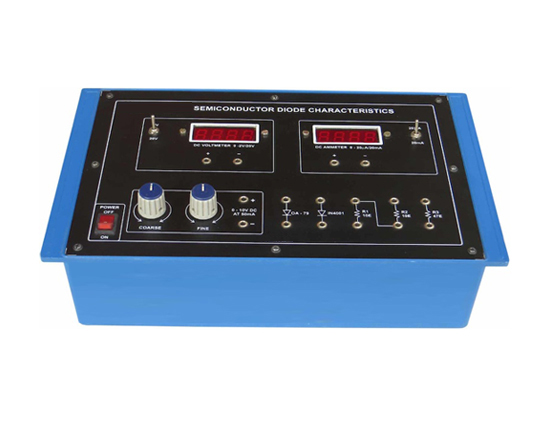
Code:EET0266
Experimental Training Board has been designed specifically for plotting Characteristics of Ge & Si Semiconductor Diodes. The board is absolutely self contained and requires no other apparatus.
Practical experience on this board carries great educative value for Science and Engineering Students.
Object:
- To Study and Plot the Forward and Reverse Bias characteristics of (Ge & Si) Semiconductor Diodes.
- To Determine the Static and Dynamic resistances of Forward Biased p-n junction of the given Diodes.
Features:
The board consists of the following built-in parts :
- 0-10V D.C. at 50mA, continuously variable with Coarse & Fine Pots, regulated Power Supply.
- D.C. Voltmeter, 65mm rectangular dial, with switch selectable ranges of 1V and 10V.
- D.C. Microammeter, 65mm rectangular dial, with switch selectable ranges of 50 mA and 10mA.
- Ge and Si Semiconductor Diodes.
- Adequate no. Of other electronic components.
- Mains ON/OFF switch, Fuse and Jewel light.
- The unit is operative on 230V ±10% at 50Hz A.C. Mains.
- Adequate no. of patch cords stackable from rear both ends 4mm spring loaded plug length ½ metre.
- Good Quality, reliable terminal/sockets are provided at appropriate places on panel for connections/ observation of waveforms.
- Strongly supported by detailed Operating Instructions, giving details of Object, Theory, Design procedures, Report Suggestions and Book References.
- Weight : 3 Kg. (Approx.)
- Dimension : W 340 x H 110 x D 210
Note: Specifications are subject to change. Order Code can be different from Manufacturer's Model No.
Study of Unijunction Transistor (U. J. T.)
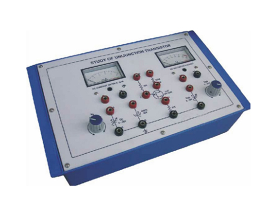
Code:EET0271
Experimental Training Board has been designed specifically to study different properties of Unijunction Transistor.
Practical experience on these boards carries great educative value for Science and Engineering Students.
Object:
- To plot V-I characteristics of a given U.J.T. (Unijunction Transistor).
- To use the given U.J.T. as a Relaxation Oscillator.
Features:
The board consists of the following built-in parts :
- Two 0-30V DC at 50mA, continuously variable regulated Power Supplies
- D.C. Voltmeter, 65mm rectangular dial to read 0-30V.
- D.C. Ammeter, 65mm rectangular dial to read 0-5mA.
- Unijunction Transistor.
- Adequate no. of other electronic components.
- Mains ON/OFF switch, Fuse and Jewel light.
- The unit is operative on 230V ±10% at 50Hz A.C. Mains.
- Adequate no. of patch cords stackable from rear both ends 4mm spring loaded plug length ½ metre.
- Good Quality, reliable terminal/sockets are provided at appropriate places on panel for connections/ observation of waveforms.
- Strongly supported by detailed Operating Instructions, giving details of Object, Theory, Design procedures, Report Suggestions and Book References.
- Weight : 3 Kg. (Approx.)
- Dimension : W 340 x H 110 x D 210
Other Apparatus Required:
- Cathode Ray Oscilloscope 20 MHz
Note: Specifications are subject to change. Order Code can be different from Manufacturer's Model No
Timer Applications IC-555 No.1
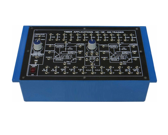
Code:EET0276
Experimental Training Board has been designed specifically to study various applications of Timer IC 555. This Training Board is useful to realise 50% Duty Cycle Oscillator, Ramp Generator, Time Delay Circuit, Sequence Generator, Schmitt Trigger, Monostable Multivibrator, Astable Multivibrator, Pulse Width Modulator, Pulse Position Modulator etc.
Practical experience on this board carries great educative value for Science and Engineering Students.
Object:
- Astable Multivibrator.
- Mono-Stable Multivibrator.
- Frequency Divider.
- Linear Ramp Generator.
- Square Wave Generator.
- Missing Pulse Detector.
- Pulse Width Modulation.
- Pulse Position Modulation.
- Schmitt Trigger.
- Sequence Generator.
- Bistable Multivibrator.
- Simple Clock Generator.
Features:
The board consists of the following built-in parts :
- +10 V at 100mA, IC regulated Power Supply.
- Sine-Square Wave Generator of 100 Hz and 1 KHz respectively, using ICs.
- Two Timer Ics 555.
- Two Diodes and one PNP transistor.
- Two Potentiometers.
- Adequate no. of other electronic components.
- Mains ON/OFF switch, Fuse and Jewel light.
- The unit is operative on 230V ±10% at 50Hz A.C. Mains.
- Adequate no. of patch cords stackable from rear both ends 4mm spring loaded plug length ½ metre.
- Good Quality, reliable terminal/sockets are provided at appropriate places on panel for connections/ observation of waveforms.
- Strongly supported by detailed Operating Instructions, giving details of Object, Theory, Design procedures, Report Suggestions and Book References.
Other Apparatus Required:
- VTVM
- Dual Trace Cathode Ray Oscilloscope 20MHz
Active Filters
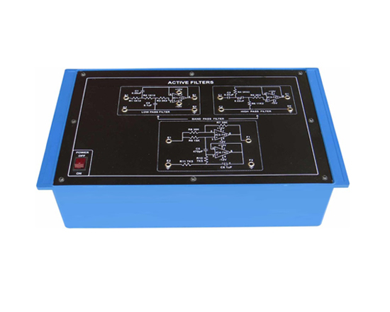
Code:EET0281
Experimental Training Board has been designed specifically to study characteristics of various types of Active Filters. This Training Board includes low pass, high pass, band pass and notch filters. The filter circuits are designed using second order Butter worth polynomials and provide unity gain in the pass band.
Practical experience on this board carries great educative value for Science and Engineering Students.
Object:
- LOW PASS FILTER
(a) Upper Cut-off frequency : 1 KHz
(b) Cut-off slope : 29.5 dB/decade
(c) Input impedance : 3.5 K at 1KHz
(d) Output impedance : 18 Ohms at 1KHz
- HIGH PASS FILTER
(a) Lower cut-off frequency : 100 Hz
(b) Cut-off slope : 26 dB/decade
(c) Input impedance : 12 K at 100 Hz
(d) Output impedance : 30 Ohms at 100 Hz
- BAND PASS FILTER
(a) Upper cut-off frequency : 1 Khz
(B) Lower cut-off frequency : 100 Hz
(c) Upper cut-off slope : 29.5 dB/decade
(d) Lower cut-off frequency : 26 dB/decade
(e) Input impedances : 24 K at 100 Hz , 3.5 K at 1 KHz
(F) Output impedances : 30 Ohms at 100 Hz, 27 Ohms at 1 Khz
- NOTCH FILTER
(A) Notch frequency : 1 KHz
(B) Input impedance : 15 K at 1 KHz
(c) Output impedance : 25 ohms at 1 KHz
(d) Notch width : 100 Hz
Features:
The board consists of the following built-in parts :
- ±12V DC at 50mA, IC regulated Power Supply internally connected.
- Four Operational Amplifier ICs.
- Adequate no. of other electronic components.
- Mains ON/OFF switch, Fuse and Jewel light.
- The unit is operative on 230V ±10% at 50Hz A.C. Mains.
- Adequate no. of patch cords stackable from rear both ends 4mm spring loaded plug length ½ metre.
- Good Quality, reliable terminal/sockets are provided at appropriate places on panel for connections/ observation of waveforms.
- Strongly supported by detailed Operating Instructions, giving details of Object, Theory, Design procedures, Report Suggestions and Book References.
- Weight : 3 Kg. (Approx.)
- Dimension : W 340 x H 110 x D 210
Other Apparatus Required:
- Decade Audio Frequency Generator
- A.C. Millivoltmeter
Note: Specifications are subject to change. Order Code can be different from Manufacturer's Model No.
MOS-FET Characteristics
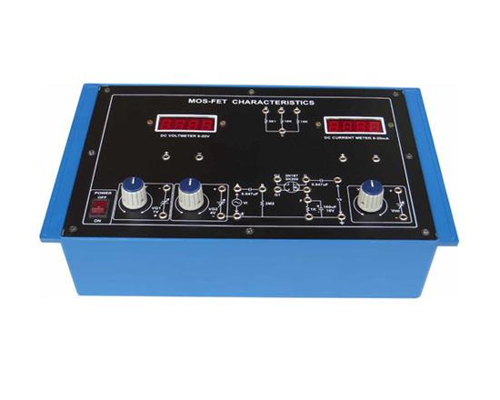
Code:EET0286
Experimental Training Board has been specifically designed to study the characteristics of MOSFET (Metal Oxide Semiconductor Field Effect Transistor) and its use as an amplifier.
Practical experience on these boards carries great educative value for Science and Engineering Students.
Object:
- To determine experimentally the Drain characteristics of a given MOSFET.
- To study the use of MOSFET as an amplifier and to measure its voltage gain in common source configuration.
Features:
The board consists of the following built-in parts :
- 0-15V D.C. at 50mA, continuously variable regulated Power Supply.
- 0-4V D.C. at 10mA, continuously variable regulated Power Supply.
- 0-1V D.C. at 10mA, continuously variable regulated Power Supply.
- D.C. Voltmeter, 65mm rectangular dial with switch selectable ranges of 1V and 15V.
- D.C. Milliammeter, 65mm rectangular dial to read 0-30mA.
- Metal Oxide Semiconductor Field Effect Transistor (MOSFET).
- Adequate no. of other electronic components.
- Mains ON/OFF switch, Fuse and Jewel light.
- The unit is operative on 230V ±10% at 50Hz A.C. Mains.
- Adequate no. of patch cords stackable from rear both ends 4mm spring loaded plug length ½ metre.
- Good Quality, reliable terminal/sockets are provided at appropriate places on panel for connections/ observation of waveforms.
- Strongly supported by detailed Operating Instructions, giving details of Object, Theory, Design procedures, Report Suggestions and Book References.
- Weight : 3 Kg. (Approx.)
- Dimension : W 340 x H 110 x D 210
Other Apparatus Required:
- Audio Frequency Generator
- A.C. Millivoltmeter
- Cathode Ray Oscilloscope 20MHz
Note: Specifications are subject to change. Order Code can be different from Manufacturer's Model No.
Junction Diode Rectifier & Filter Characteristics
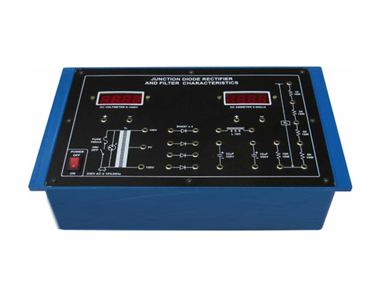
Code:EET0291
Experimental Training Board has been designed specifically for the Study of the Junction Diode Rectifier and Filter Characteristics.
Practical experience on these boards carries great educative value for Science and Engineering Students.
Object:
- Study of Junction Diode Rectifier output and ripple content for different resistive loads for :
(a) Half wave.
(b) Full wave (Centre Tap).
(c) Full wave (Bridge).
(d) Voltage Doubler Circuit
- Study of filter and load regulation characteristics for half wave and full wave rectifier having different resistive loads and filters of the type
(a) Capacitor filter.
(b) Capacitor Filter with capacitor value doubled.
(c) Inductor filter.
(d) Capacitor input L section filter.
(e) Capacitor input p section filter.
Features:
The board consists of the following built-in parts :
- Mains transformer, secondary centre tap 100-0-100V at 100 mA.
- DC Milliammeter, 65mm rectangular dial to read 0-100 mA.
- DC Voltmeter, 65mm rectangular dial to read 0-300 V.
- Four Silicon Junction Diodes.
- Filter choke.
- Adequate no. of other electronic components.
- Mains ON/OFF switch, Fuse and Jewel light.
- The unit is operative on 230V ±10% at 50Hz A.C. Mains.
- Adequate no. of patch cords stackable from rear both ends 4mm spring loaded plug length ½ metre.
- Good Quality, reliable terminal/sockets are provided at appropriate places on panel for connections/ observation of waveforms.
- Strongly supported by detailed Operating Instructions, giving details of Object, Theory, Design procedures, Report Suggestions and Book References.
- Weight : 3 Kg. (Approx.)
- Dimension : W 340 x H 110 x D 210
Other Apparatus Required:
Note: Specifications are subject to change. Order Code can be different from Manufacturer's Model No.
Charging and Discharging of a Condenser
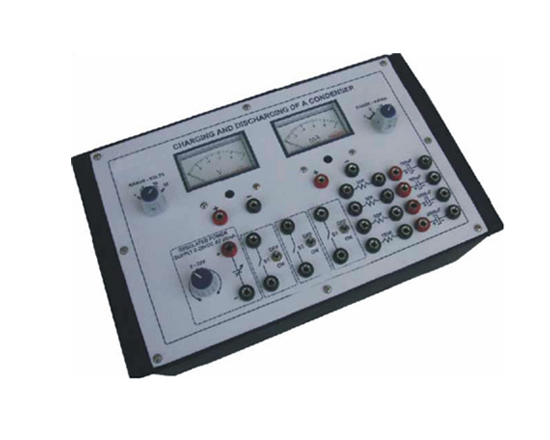
Code:EET0296
Experimental Training Board has been specifically designed to study Charging and Discharging of a Condenser.
Practical experience on these boards carries great educative value for Science and Engineering Students.
Object:
- To study the charging of a condenser, to plot a graph of voltage (V) across it against time (t) and to determine the time constant from this graph.
- To plot a graph of charging current (i) against time (t) and to determine the time constant from this graph.
- To study the discharging of a condenser, to plot a graph of voltage (V) across the condenser against time (t) and to determine the time constant from this graph.
- To plot a graph of discharge current (i) against time (t) and to determine the time constant from this graph.
Features:
The board consists of the following built-in parts :
- 0-20V D.C. at 25 mA, continuously variable regulated Power Supply.
- D.C Voltmeter, 65mm rectangular dial with switch selectable ranges of 1,5,10 and 25 volts.
- D.C. Milliammeter, 65mm rectangular dial with switch selectable ranges of 1,5,10 and 25 mA.
- Three SPST switches.
- Four electrolytic condensers.
- Adequate no. of other electronic components.
- Mains ON/OFF switch, Fuse and Jewel light.
- The unit is operative on 230V ±10% at 50Hz A.C. Mains.
- Adequate no. of patch cords stackable from rear both ends 4mm spring loaded plug length ½ metre.
- Good Quality, reliable terminal/sockets are provided at appropriate places on panel for connections/ observation of waveforms.
- Strongly supported by detailed Operating Instructions, giving details of Object, Theory, Design procedures, Report Suggestions and Book References.
- Weight : 3 Kg. (Approx.)
- Dimension : W 340 x H 110 x D 210
Other Apparatus Required:
Note: Specifications are subject to change. Order Code can be different from Manufacturer's Model No.
Semiconductor Devices Characteristics
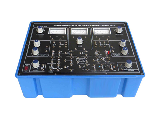
Code:EET0301
Experimental Training Board has been designed specifically to study the Characteristics of a large family of Semiconductor Devices.
Practical experience on these boards carries great educative value for Science and Engineering Students.
Object:
- Germanium and Silicon Diodes.
- Zener Diodes.
- Transistor ( Bipolar ) PNP and NPN.
- Field Effect Transistor (FET).
- Uni-Junction Transistor (UJT).
- Light Emitting Diode (LED).
- Photo Diode.
- Photo Transistor .
- Thermistors N.T.C. and P.T.C.
- Voltage Dependant Resistor (V.D.R.).
- Light Dependant Resistor (L.D.R.).
- Opto-Coupler.
- DIAC.
- Silicon Controlled Rectifier (SCR).
- TRIAC.
- Varactor Diode ( Varicap Diode).
Features:
The board consists of the following built-in parts :
- Two, 0-1.5V DC, 0-10V DC and 0-25V DC at 500mA, IC Regulated Power Supplies (switch selectable).
- 0-50V D.C. at 100mA,continuously variable regulated Power Supply.
- Two, D.C. Ammeters, 65mm rectangular dial with switch selectable ranges of 50mA, 500mA, 5mA, 50mA and 500mA.
- D.C. Voltmeter,65mm rectangular dial with switch selectable ranges of 1V,10V and 50V.
- Electronic devices (all as mentioned under heading "OBJECT").
- Adequate no. of other electronic components.
- Mains ON/OFF switch, Fuse and Jewel light.
- The unit is operative on 230V ±10% at 50Hz A.C. Mains
- Adequate no. of patch cords stackable from rear both ends 4mm spring loaded plug length ½ metre.
- Good Quality, reliable terminal/sockets are provided at appropriate places on panel for connections/ observation of waveforms.
- Strongly supported by detailed Operating Instructions, giving details of Object, Theory, Design procedures, Report Suggestions and Book References.
- Weight : 7 Kg. (Approx.)
- Dimension : W 412 x H 150 x D 310
Other Apparatus Required:
- Digital Capacitance Meter
Note: Specifications are subject to change. Order Code can be different from Manufacturer's Model No.
Discrete Component Trainer
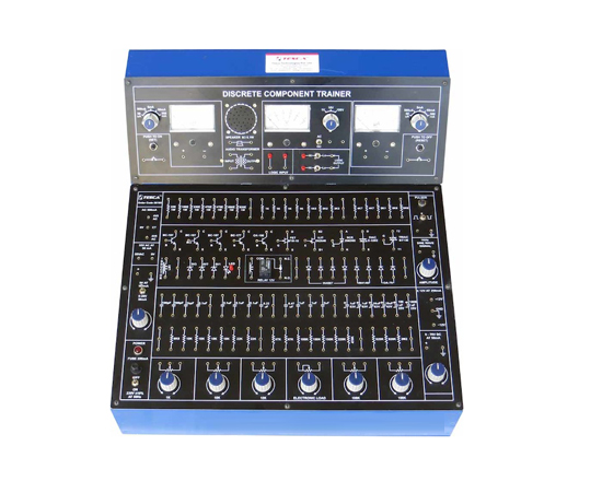
Code:EET0306
Experimental Training Board has been designed specifically for the study of Discrete Electronic Components. It contains a wide selection of discrete components and A.C. & D.C. Power Supplies. The capabilities of this trainer extend far beyond the experiments described. Although only a finite number of experiments have been described yet other circuits as per individuals requirements can also be designed using the available components and power supplies.
Practical experience on these boards carries great educative value for Science and Engineering Students.
Object:
- RC & LC CIRCUITS :
01. Study of RC High Pass Filter
02. Study of RC Low Pass Filter
03. Study of RL Differentiating Circuits
04. Study of Series RC Circuit
05. Study of Series LC Circuit
06. Study of Parallel RC Circuit
07. Study of Parallel LC Circuit
- SERIES & PARALLEL RESONANCE CIRCUIT :
01. Study of Series LCR Resonance Circuit and determination of 'Q'
02. Study of Parallel LCR Resonance Circuit
03. Determination of impedance & reactance of reactive elements and plotting of reactive curves
- GERMANIUM & SILICON DIODES :
01. Characteristics of a germanium diode
02. Characteristics of a silicon diode
03. Application of a diode as a half wave rectifier
04. Application of four diodes as full wave bridge rectifier
- ZENER DIODE :
01. Characteristics of a Zener Diode
02. Application of a Zener Diode as a voltage regulator
03. Determination of line regulation of a zener diode regulator circuit
04. Determination of load regulation of a zener diode regulator circuit
- CLIPPING & CLAMPING CIRCUITS :
01. Study of single level clipping circuits
02. Study of two level clipping circuits
03. Study of clamping circuits
- COMMON EMITTER CONFIGURATION OFATRANSISTOR :
01. Input characteristics of common emitter configuration
02. Output characteristics of common emitter configuration
03. Study of common emitter amplifier
- COMMON BASE CONFIGURATION OF ATRANSISTOR:
01. Input characteristics of common base configuration
02. Output characteristics of common base configuration
03. Study of common base amplifier
- COMMON COLLECTOR CONFIGURATION OFATRANSISTOR :
01. Transfer characteristics of common collector configuration
- EMITTER FOLLOWER ( TRANSISTOR) :
01. Study of emitter follower configuration
- CASCADED AMPLIFIER :
01. Study of two stage cascaded amplifier
- POWER AMPLIFIER
01. Study of class-A power amplifier
- DIFFERENTIAL AMPLIFIER :
01. Study of a differential amplifier and determination of its CMRR
- FEED BACK AMPLIFIER
01. Study of current series feedback
02. Study of current shunt feedback
- SELECTIVE AMPLIFIER :
01. Study of frequency selective amplifier
- FET CHARACTERISTICS & SOURCE FOLLOWER:
01. Study of static characteristics of an FET
02. Application as source follower
- FET CHOPPER & V.V.R. (Voltage Variable Resistor)
01. Application as a Chopper
02. Application as Voltage Variable Resistor (VVR)
- R.C. PHASE SHIFT OSCILLATOR :
01. Study of R.C. Phase Shift Oscillator
- U.J.T. CHARACTERISTICS & RELAXATION OSCILLATOR :
01. Study of UJT Characteristics
02. Application of UJT as relaxation oscillator
- TRIAC CHARACTERISTICS :
01. Terminal Characteristics in Mode I+
02. Terminal Characteristics in Mode III+
03. Measurement of Holding Current IH
04. Gate characteristics in Mode I+
05. Gate characteristics in Mode I-
06. Gate characteristics in Mode III+
07. Gate characteristics in Mode III-
08. Application in power control using D.C. control voltage
09. Application in power control using A.C. control voltage
- BISTABLE MULTIVIBRATOR :
01. Study of bistable multivibrator circuit
- MONOSTABLE MULTIVIBRATOR :
01. Study of monostable multivibrator circuit
- ASTABLE MULTIVIBRATOR :
01. Study of astable multivibrator circuit
- SCHMITTTRIGGER :
01. Study of Schmitt Trigger circuit
- BASIC LOGIC GATES :
01. Study of AND gate
02. Study of OR gate
03. Study of NAND gate
04. Study of NOR gate
- LED CHARACTERISTICS & APPLICATIONS :
01. Study of Characteristics of LED
02. Application of LED in constant current sources
- SCR CHARACTERISTICS :
01. D.C. gate control characteristics
02. Anode current characteristics
- DIAC CHARACTERISTICS & APPLICATIONS :
01. Study of Characteristics of a Diac
02. Application as sawtooth wave & pulse generator
03. Application in Diac Triac Power control circuit
Features:
The board consists of the following built-in parts :
- 4V5-0-4V5 A.C. at 500 mA, Power Supply.
- 0-5VA.C. at 50mA, Power Supply.
- 0-70V D.C. at 50 mA, continuously variable Power Supply.
- ± 12V D.C. at 250 mA, IC regulated and short circuit protected Power Supply.
- 0-20V D.C. at 50 mA, IC Regulated Power Supply.
- 5V D.C. at 100mA, IC Regulated Power Supply.
- A.C. / D.C. Voltmeter, 65mm rectangular dial, with switch selectable ranges of 1V, 10V and 100V.
- Two D.C. Ammeters, 65mm rectangular dial, with switch selectable ranges of 50 mA/500mA/5mA/50mA/500mA.
- Pulser with Dual Polarity, selectable output.
- 1 KHz Sine wave source with variable output level.
- LEDs for visual indication of Input & Output status.
- Speaker, LED, 8 diodes, 5 Zener diodes, Diac, SCR, Triac, 2 FET, UJT, 7 Transistors, 1 matched transistor pair, 67 resistors, 27 capacitors, 6 potentiometers, Electronic Load, indicator, Audio Transformer.
- 12 V, OEN Relay with one change over contacts rated at 6 Amp. for resistive and 3 Amp. for inductive Load at 230V.
- Mains ON/OFF switch, fuse and Neon Indicator are provided.
- The unit is operative on 230V ±10% at 50Hz A.C. Mains.
- 13. 12 V, OEN Relay with one change over contacts rated at 6 Amp. for resistive and 3 Amp. for inductive Load at 230V.
- Adequate no. of patch cords stackable from rear both ends 4mm spring loaded plug length ½ metre.
- Good Quality, reliable terminal/sockets are provided at appropriate places on panel for connections/ observation of waveforms.
- Strongly supported by detailed Operating Instructions, giving details of Object, Theory, Design procedures, Report Suggestions and Book References.
Other Apparatus Required:
- Sine Square Wave Oscillator
- Cathode Ray Oscilloscope 20MHz
Voltage Regulator IC 723
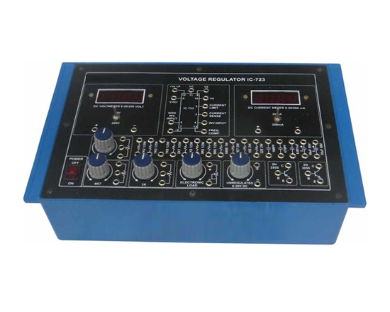
Code:EET0311
Experimental Training Board has been designed specifically to study Voltage Regulator IC 723. This Training Board gives a thorough understanding of the basic parameters of IC 723, their measurement and also covers useful applications of this regulator IC. The board is absolutely self contained and requires no other apparatus.
Practical experience on these boards carries great educative value for Science and Engineering Students.
Object:
- To study and measure the following parameters of IC 723 :
- Load Regulation.
- Line Regulation.
- To study the following applications :
- Low voltage regulator circuit 2 to 7V.
- High voltage regulator circuit 7 to 27V.
- Voltage regulator with increased current capability using external NPN power transistor.
- Voltage regulator with increased current capability using external PNP power transistor.
- Voltage regulator with fold back current limiting.
- Negative voltage regulator.
Features:
- 0-35V D.C. at 250mA, countinously variable unregulated Power Supply.
- D.C. Milliammeter, 65mm Rectangular dial with switch selectable ranges of 50mA and 250mA.
- D.C. Voltmeter, 65mm rectangular dial with switch selectable ranges of 10V and 40V.
- IC 723 fitted on base.
- Three Potentiometers.
- Electronic load.
- NPN Power transistor.
- PNP Power transistor.
- Adequate no. of other electronic components
- Mains ON/OFF switch, Fuse and Jewel light.
- The unit is operative on 230V ±10% at 50Hz A.C. Mains.
- Adequate no. of patch cords stackable from rear both ends 4mm spring loaded plug length ½ metre.
- Good Quality, reliable terminal/sockets are provided at appropriate places on panel for connections/ observation of waveforms.
- Strongly supported by detailed Operating Instructions, giving details of Object, Theory, Design procedures, Report Suggestions and Book References.
Phase Locked Loop IC-565
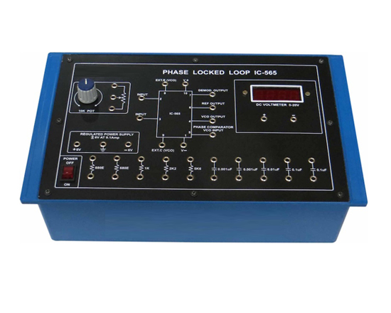
Code:EET0316
Experimental Training Board has been designed specifically for the study of Phase Locked Loop (PLL) IC 565. This training board covers most of the important parameters, characteristics and applications on Phase-locked Loop (PLL) IC 565.
Practical experience on these boards carries great educative value for Science and Engineering Students.
Object:
- VCO Characteristics :
- To study and measure the free running frequency or centre frequency of VCO.
- To study the VCO sensitivity
- To study the VCO linearity PLL Characteristics
- To study and measure the capture range and lock range.
- PLL Applications :
- Frequency synthesis
- F.M. De-modulation
- A.M. De-modulation
Features:
The board consists of the following built-in parts :
- ± 6V D.C. at 100mA, IC regulated Power Supply.
- D.C. Voltmeter, 65mm rectangular dial, with switch selectable of ranges 1V and 10V.
- Phase locked loop IC-565
- Two sets of three inter connected sockets for multi-connections wherever required.
- Adequate no. of other electronic components.
- Mains ON/OFF switch, Fuse and Jewel light.
- The unit is operative on 230V ±10% at 50Hz A.C. Mains.
- Adequate no. of patch cords stackable from rear both ends 4mm spring loaded plug length ½ metre.
- Good Quality, reliable terminal/sockets are provided at appropriate places on panel for connections/ observation of waveforms.
- Strongly supported by detailed Operating Instructions, giving details of Object, Theory, Design procedures, Report Suggestions and Book References.
Other Apparatus Required:
- Sine Square Wave Generator
- Digital frequency counter, 6 digit
- Cathode Ray Oscilloscope 20MHz
Hybrid Parameters of a Transistor
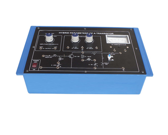
Code:EET0321
Experimental Training Board has been designed specifically for the study of Hybrid Parameters of a transistor and to derive Z and Y parameters from the hybrid- parameter results.
Practical experience on these boards carries great educative value for Science and Engineering Students.
Object:
- To measure the hybrid-parameters i.e. H11 , h12, h21 & h 22 of a transistor, at 1 KHz and at different collector current values.
- To derive Z and Y parameters from the hybrid parameter results.
Features:
The board consists of the following built-in parts :
- 0-2V5 D.C. at 100 mA, continuously variable Power Supply.
- 0-9V D.C. at 100mA, continuously variable Power Supply.
- D.C. Milliammeter, 65mm rectangular dial to read 0-10mA.
- 1 KHz Sine Wave source with variable output level 0-1V.
- PNP Germanium transistor
- Adequate no. of other electronic components.
- Mains ON/OFF switch, Fuse and Jewel light.
- The unit is operative on 230V ±10% at 50Hz A.C. Mains.
- Adequate no. of patch cords stackable from rear both ends 4mm spring loaded plug length ½ metre.
- Good Quality, reliable terminal/sockets are provided at appropriate places on panel for connections/ observation of waveforms.
- Strongly supported by detailed Operating Instructions, giving details of Object, Theory, Design procedures, Report Suggestions and Book References.
Other Apparatus Required:
Oscillators
Code:EET0326
Experimental Training Board has been designed specifically on sinusoidal Oscillators. In this training board all the basic sinusoidal oscillator circuits can be quickly and easily assembled and studied.
Practical experience on these boards carries great educative value for Science and Engineering Students.
Object:
- To study R.C. Phase Shift Oscillator of phase advance type.
- To study R.C. Phase Shift Oscillator of phase retard type.
- To study Wien-Bridge Oscillator.
- To study Hartely's Oscillator.
- To study Colpitt's Oscillator.
- To study Pierce (X-Tal) Oscillator.
- To study method of frequency measurement using a CRO.
Features:
The board consists of the following built-in parts :
- +9V D.C at 100mA, IC Regulated Power Supply.
- Two stage buffer/amplifier using PNP transistors and controllable A.C. gain.
- NPN Transistor biased in Class A common emitter configuration.
- Wien-bridge network.
- R.C. Phase Shift Net-work (advance type & retard type).
- Tank circuits for Hartley's & Colpitt's Oscillators.
- 3.579 MHz X-tal with series trimmer.
- Adequate no. of other electronic components.
- Mains ON/OFF switch, Fuse and Jewel light.
- The unit is operative on 230V ±10% at 50Hz A.C. Mains.
- Adequate no. of patch cords stackable from rear both ends 4mm spring loaded plug length ½ metre.
- Good Quality, reliable terminal/sockets are provided at appropriate places on panel for connections/ observation of waveforms.
- Strongly supported by detailed Operating Instructions, giving details of Object, Theory, Design procedures, Report Suggestions and Book References.
Other Apparatus Required:
- Cathode Ray Oscilloscope 20MHz
Multivibrators (Solid State)
Code:EET0331
Experimental Training Board has been designed specifically for the study of Multivibrator circuits. Apart from basic circuits some special techniques have also been included.
Practical experience on these boards carries great educative value for Science and Engineering Students.
Object:
- Design of multivibrators.
- To study the waveforms of a free running multivibrator.
- To design and make a bistable multivibrator and to study its D.C. conditions.
- To design and make a monostable multivibrator and to adjust its delay time.
- To design and make schmitt-trigger and study its hysteresis.
- To control the frequency of a free running multivibrator with applied voltage.
- To design and make a gated free running multivibrator.
- To design and make an improved free running multivibrator.
Features:
The board consists of the following built-in parts :
- ±9V D.C. at 100mA, IC regulated Power Supply.
- 0-9V D.C. at 5mA, IC regulated Power Supply.
- D.C. Voltmeter, 65mm rectangular dial to read 0-10V.
- Pulser for triggering the circuit.
- Three NPN transistors.
- Adequate no. of other electronic components.
- Mains ON/OFF switch, Fuse and Jewel light.
- The unit is operative on 230V ±10% at 50Hz A.C. Mains.
- Adequate no. of patch cords stackable from rear both ends 4mm spring loaded plug length ½ metre.
- Good Quality, reliable terminal/sockets are provided at appropriate places on panel for connections/ observation of waveforms.
- Strongly supported by detailed Operating Instructions, giving details of Object, Theory, Design procedures, Report Suggestions and Book References.
- Weight : 3 Kg. (Approx.)
- Dimension : W 412 x H 150 x D310
Other Apparatus Required:
- Cathode Ray Oscilloscope 20MHz
Note: Specifications are subject to change. Order Code can be different from Manufacturer's Model No.
Operational Amplifier Trainer
Code:EET0336
"OP-AMP DESIGNER" has been designed specifically for the study of OP-AMP IC and its applications. This training board covers nearly all possible applications of operational amplifiers IC and makes the student familiar with the fundamentals of OP-AMPS, their characteristics and applications in various fields.100 experiments can be performed by this OP-AMP designer.
Practical experience on these boards carries great educative value for Science and Engineering Students.
Object:
- BASIC OPERATIONAL AMPLIFIER CIRCUIT
01. Inverting Amplifier
02. Non-inverting Amplifier
03. Inverting A.C. Amplifier
04. Non-inverting A.C. Amplifier
05. High input impedance inverting Amplifier
06. High input impedance non-inverting amplifier
- SOURCE FOLLOWERS
01. Voltage Follower (Unit gain buffer amplifier)
02. A.C. Voltage follower
- OP- AMPS AS ANALOGUE COMPUTER ELEMENTS
01. Inverting summing amplifier
02. Non-inverting summing amplifier
03. Subtractor
04. Differential amplifier
05. A.C. differential amplifier
06. Adder subtractor
07. Multiplication by a constant
08. Division by a constant
09. Integrating amplifier for DC input signals
10. Integrating amplifier for AC input signals
11. Differentiator amplifier
12. Non-inverting differentiator
- FUNCTION GENERATOR
01. Sine Wave generator using wien bridge network
02. Square Wave generator
03. Pulse generator
04. Square and Triangular wave generator
05. Saw tooth generator
06. Synchronised sawtooth generator with negative going pulse trigger
07. Synchronised sawtooth generator with positive going pulse trigger
- MULTIVIBRATORS
01. Astable multivibrator
02. Monostable multivibrator
03. Bistable multivibrator
- FILTERS
01. Low pass active filter
02. High pass active filter
03. Band pass active filter
04. Notch filter
- VOLTAGE AND CURRENT REGULATOR
01. Basic reference voltage source
02. Basic reference voltage source with buffered output
03. Basic reference voltage source with negative output
04. Negative voltage reference source with buffered output
05. Positive regulator with variable buffered output
06. Negative regulator with variable buffered output
07. Buffered reference source
08. Basic non-inverting voltage controlled current source
- SIGN CHANGER
01. Sign changer with variable output
02. Switch select sign changer
- PHASE SHIFT CIRCUIT
01. Constant amplitude lag circuit
02. Constant amplitude lead circuit
- SIGNAL PROCESSING CIRCUITS
01. Diodes
- Precision Diode with +O/P
- Precision Diode with -O/P
02. Rectifier
- Half wave rectifier
- Full wave rectifier
- Filtered full wave rectifier
03. Detectors
- Peak detector
- Buffered peak detector
- Inverting peak detector
- Zero crossing detector
- Buffered zero crossing
04. Clippers
- Positive peak clipper
- Negative peak clipper
- Self buffered series clipper
- Shunt clipper
- DC restorer
05. Dead Band Response
- Feed back circuit with dead band response
- Variable dead band circuit
- LIMITERS
01. General purpose unipolar limiter
02. Bipolar zener limiter
03. Input current limiter
04. Diode bridge limiter using one zener
05. Adjustable bipolar limiter
- COMPARATORS
01. Fast precision voltage comparator
02. Single ended comparator with hysteresis & clamped feed back
03. Comparator for signals of opposite polarity
04. Comparator for A.C. coupled signals
- INSTRUMENTATION AMPLIFIER
01. Basic differential input instrumentation amplifier
02. Instrumentation amplifier with high input impedance
- OUTPUT DISPLAYS FOR COMPARATOR
01. LED driver
02. Lamp driver
- METERING CIRCUITS
01. D.C. voltmeter
02. D.C. ammeter
03. Resistance to voltage converter
- LATCH UP PROTECTION
01. Elimination of latch up
- PUSH PULL CONVERSION
01. Single ended to push pull conversion
- MODULATION
1. Pulse amplitude modulation
- OFF-SET ADJUSTMENT IN OP-AMP CIRCUITS
01. Internal off set Nulling
- For inverting amplifier
- For non-inverting amplifier
- For voltage follower
02. Universal External off set Nulling
- Inverting amplifier offset voltage applied to the inverting input
- Inverting amplifier offset voltage applied to the noninverting input
- Off-setting circuit for low gain non-inverting amplifier
- Off-setting circuit for high gain non-inverting amplifier
- Off-setting circuit for voltage follower
03. Other types of off-setting arrangements
- Zero off-setting
- Zero off-setting buffer
- MEASUREMENT OF OP-AMP PARAMETERS
01. Measurement of closed loop gain
02. Measurement of closed loop-r (inverting mode) in
03. Measurement of closed loop-r (non-inverting mode) in
04. Measurement of O/P resistance (closed loop)
05. Measurement of Band width of ac amplifier
06. Input off-set voltage
07. Input bias current
08. Input off-set current
Features:
The board consists of the following built-in parts :
- IC Regulated D.C. Power Supply.
- Continuously variable D.C. Power Supply.
- Two OP-Amp IC.
- Transistor, 5 diodes, 2 zener diodes, 28 resistors, 8 capacitors, one LED, one lamp.
- Mains ON/OFF switch, fuse and Neon Indicator are provided.
- The unit is operative on 230V ±10% at 50Hz A.C. Mains.
- Adequate no. of patch cords stackable from rear both ends 4mm spring loaded plug length ½ metre.
- Good Quality, reliable terminal/sockets are provided at appropriate places on panel for connections/ observation of waveforms.
- Strongly supported by detailed Operating Instructions, giving details of Object, Theory, Design procedures, Report Suggestions and Book References.
- Weight : 5 Kg. (Approx.)
- Dimension : W 412 x H 150 x D 310
Other Apparatus Required:
- Sine Square Wave Oscillator
- Digital Multimeter 3¾ digit
- A.C. Millivoltmeter
- Cathode Ray Oscilloscope 20MHz
Note: Specifications are subject to change. Order Code can be different from Manufacturer's Model No.
Zener Regulated Power Supplies
Code:EET0341
Experimental Training Board has been designed specifically for the study of regulated power supplies based on Zener Voltage regulating diodes. A Zener diode is generally employed in a standard circuit as a voltage regulator. This training board deals with some more possible voltage regulating circuits apart from the standard one. The board is absolutely self contained and requires no other apparatus.
Practical experience on these boards carries great educative value for Science and Engineering Students.
Object:
- To study the standard zener diode voltage regulated power supply.
- To study the zener diode voltage regulated supply having two zener diodes in series.
- To study a dual polarity voltage regulated supply employing two zener diodes.
- To study a zener diode voltage regulated supply employing a series pass transistor for increasing the output current capability of the circuit.
Features:
The board consists of the following built-in parts :
- ± 12V5 ± 10% at 50mA, unregulated D.C. Voltage.
- D.C. Voltmeter, 65mm rectangular dial to read 0-15V.
- DC Milliammeter, 65mm rectangular dial to read 0-50mA.
- NPN Transistor.
- Three zener diodes.
- Adequate no. of other electronic components.
- Mains ON/OFF switch, Fuse and Jewel light.
- The unit is operative on 230V ±10% at 50Hz A.C. Mains.
- Adequate no. of patch cords stackable from rear both ends 4mm spring loaded plug length ½ metre.
- Good Quality, reliable terminal/sockets are provided at appropriate places on panel for connections/ observation of waveforms.
- Strongly supported by detailed Operating Instructions, giving details of Object, Theory, Design procedures, Report Suggestions and Book References.
Comparative Study of CE, CB And CC Amplifiers
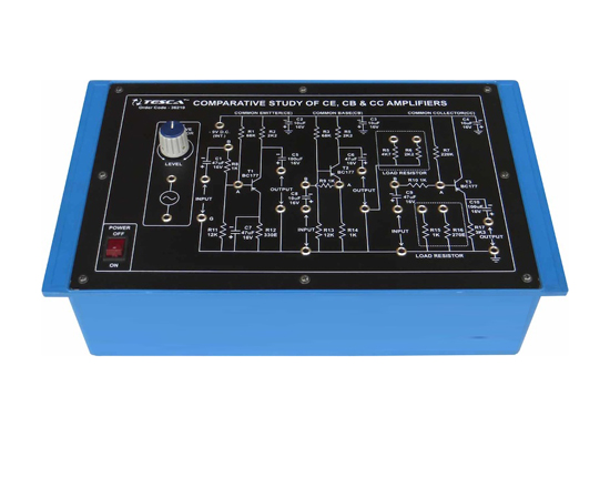
Code:EET0346
Experimental Training Board has been designed specifically for the Comparative study of Common Emitter (CE), Common Base (CB) and Common Collector (CC) Transistor Amplifiers. These practical transistor amplifier configurations are evaluated in respect of their main parameters and results are compared with theoretical calculations.
Practical experience on these boards carries great educative value for Science and Engineering Students.
Object:
- Study of Common Emitter (CE) transistor amplifier circuit and evaluation of its input & output resistance, voltage gain, current gain and power gain.
- Study of Common Base (CB) transistor amplifier circuit and evaluation of its input and output resistance, voltage gain, current gain and power gain.
- Study of Common Collector (CC) transistor amplifier circuit and evaluation of its input and output resistance, voltage gain, current gain and power gain.
Features:
The board consists of the following built-in parts :
- ± 9V D.C. at 100mA, IC Regulated Power Supply internally connected.
- All the three circuits i.e. CE, CB and CC are built separately.
- Adequate no. of other electronic components.
- Sine Wave Signal Generator of 1KHz, with variable level, low distortion, based on IC.
- Mains ON/OFF switch, Fuse and Jewel light.
- The unit is operative on 230V ±10% at 50Hz A.C. Mains.
- Adequate no. of patch cords stackable from rear both ends 4mm spring loaded plug length ½ metre.
- Good Quality, reliable terminal/sockets are provided at appropriate places on panel for connections/ observation of waveforms.
- Strongly supported by detailed Operating Instructions, giving details of Object, Theory, Design procedures, Report Suggestions and Book References.
Other Apparatus Required:
- A.C. Millivoltmeter
- Cathode Ray Oscilloscope 20MHz
Study of Diode Clipping Circuits
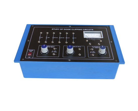
Code:EET0351
Experimental Training Board has been designed specifically to study eight different types of circuits for single level and two level clipping for an input sine wave signal.
Practical experience on these boards carries great educative value for Science and Engineering Students.
Object:
- To study diode clipping circuits.
- Single level clipping circuits :
- Positive base clipping with diode in series.
- Positive base clipping with diode in shunt.
- Negative base clipping with diode in series.
- Negative base clipping with diode in shunt.
- Negative peak clipping.
- Positive peak clipping.
- Two level clipping circuits :
- Two level clipping with diodes.
- Two level clipping with zener diodes.
Features:
The board consists of the following built-in parts :
- Two, 0-10V D.C. at 10mA, continuously variable Power Supplies.
- 0-12V, A.C. 50Hz at 20mA, continuously variable Power Supply.
- D.C. Voltmeter, 65mm rectangular dial to read 0-10V.
- Two silicon diodes.
- Two zener diodes./li>
- Adequate no. of other electronic components.
- Mains ON/OFF switch, Fuse and Jewel light.
- The unit is operative on 230V ±10% at 50Hz A.C. Mains.
- Adequate no. of patch cords stackable from rear both ends 4mm spring loaded plug length ½ metre.
- Good Quality, reliable terminal/sockets are provided at appropriate places on panel for connections/ observation of waveforms.
- Strongly supported by detailed Operating Instructions, giving details of Object, Theory, Design procedures, Report Suggestions and Book References.
Other Apparatus Required:
- Decade Audio Frequency Generator
- Cathode Ray Oscilloscope 20MHz
Opto Electronic Devices Characteristics
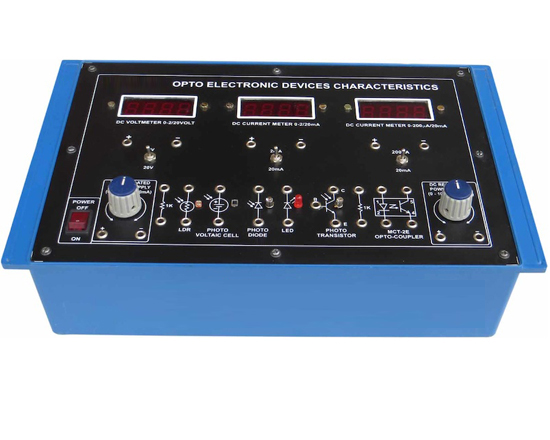
Code:EET0356
Experimental Training Board has been designed specifically to study the characteristics of Opto Electronic Devices. Different experiments have been included in this Opto Electronic Devices characteristics board in order that a wide range of topics on Opto Electronics Devices Characteristics be covered in a short span of time. All the circuits for obtaining the characteristics of various devices can be easily assembled on this versatile training board itself.
Practical experience on these boards carries great educative value for Science and Engineering Students.
Object:
- Light Emitting Diode (LED).
- Photo Diode.
- Photo Transistor.
- Light Dependent Resistor (L.D.R.).
- Photo Voltaic Cell.
- Optocoupler.
Features:
The board consists of the following built-in parts :
- Two 0-10V D.C. at 100mA, continuously variable regulated Power Supplies.
- D.C. Milliammeter, 65mm rectangular dial to read 0-10mA.
- D.C Microammeter, 65mm rectangular dial, with switch selectable ranges of 50mA, 500mA, 5mA and 50mA.
- D.C. Voltmeter, 65mm rectangular dial, with switch selectable ranges of 1V and 10V.
- Opto Electronic Devices:
- Light Emitting Diode (LED)
- Photo Diode
- Photo Transistor
- Light Dependent Resistance (LDR)
- Photo Voltaic Cell
- Opto Coupler
- Adequate no. of other electronic components.
- The unit is operative on 230V ±10% at 50Hz A.C. Mains.
- Adequate no. of patch cords stackable from rear both ends 4mm spring loaded plug length ½ metre.
- Good Quality, reliable terminal/sockets are provided at appropriate places on panel for connections/ observation of waveforms.
- Strongly supported by detailed Operating Instructions, giving details of Object, Theory, Design procedures, Report Suggestions and Book References.
- Weight : 3 Kg. (Approx.)
- Dimension : W 340 x H 110 x D 210
Other Apparatus Required:
- Variac 0-230V, 50Hz at 2 Amp
- 40 Watts, table lamp
Note: Specifications are subject to change. Order Code can be different from Manufacturer's Model No.
Time Delay Relay
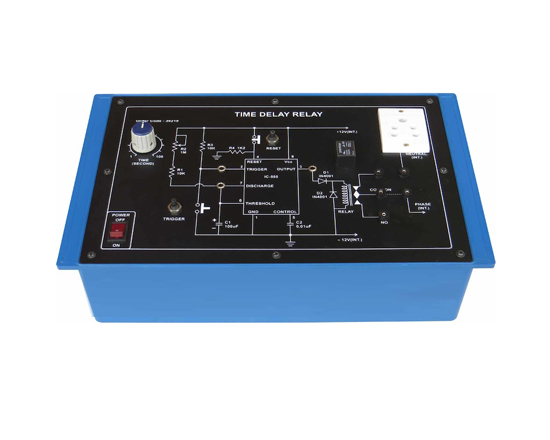
Code:EET0361
Experimental Training Board has been designed specifically for the study of Time Delay Relay circuit. This training board can also be used as a time delay relay to control external loads. The board is absolutely self contained and requires no other apparatus.
Practical experience on these boards carries great educative value for Science and Engineering Students.
Object:
- To study the time delay relay circuit with controlling ON time.
- To study the time delay relay circuit with controlling OFF time.
Features:
The board consists of the following built-in parts :
- +12V D.C. at 100mA, IC regulated Power Supply internally connected.
- Relay 12V D.C. having single pole, 2 way, to control ON time as well as OFF time, connected internally with circuit.
- Provision for varying the delay time i.e. time can be set from 1 sec to 100 sec.
- Trigger & Reset switches.
- 15 W pigmy lamp to demonstrate the relay operation.
- Circuit based on timer IC.
- Adequate no. of other electronic components.
- Mains ON/OFF switch, Fuse and Jewel light.
- The unit is operative on 230V ±10% at 50Hz A.C. Mains.
- Adequate no. of patch cords stackable from rear both ends 4mm spring loaded plug length ½ metre.
- Good Quality, reliable terminal/sockets are provided at appropriate places on panel for connections/ observation of waveforms.
- Strongly supported by detailed Operating Instructions, giving details of Object, Theory, Design procedures, Report Suggestions and Book References.
Verification of Ohm's Law Series & Parallel Circuits
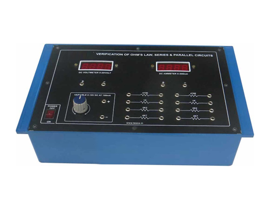
Code:EET0366
Experimental Training Board has been designed specifically for the verification of Ohm's Law & to study the series and parallel combination of Resistance network. This training board is quite useful for imparting the basic knowledge of voltage and current distribution and the effect of series parallel circuit. The board is absolutely self contained and requires no other apparatus.
Practical experience on these boards carries great educative value for Science and Engineering Students.
Object:
- Verification of ohm's Law.
- To study series circuits.
- To study parallel circuits.
Features:
The board consists of the following built-in parts :
- 0-15 VD.C. at 100 mA, continuously variable regulated Power Supply.
- D.C. Voltmeter, 65mm rectangular dial to read 0-15V D.C.
- D.C. Milliammeter, 65mm rectangular dial to read 0-50mA D.C.
- Adequate no. of other electronic components.
- Mains ON/OFF switch, Fuse and Jewel light.
- The unit is operative on 230V ±10% at 50Hz A.C. Mains.
- Adequate no. of patch cords stackable from rear both ends 4mm spring loaded plug length ½ metre.
- Good Quality, reliable terminal/sockets are provided at appropriate places on panel for connections/ observation of waveforms.
- Strongly supported by detailed Operating Instructions, giving details of Object, Theory, Design procedures, Report Suggestions and Book References.
- Weight : 3 Kg. (Approx.)
- Dimension : W 340 x H 110 x D 210
Note: Specifications are subject to change. Order Code can be different from Manufacturer's Model No.
Measurement of Inductance & Capacitance by Maxwell's L/C Bridge
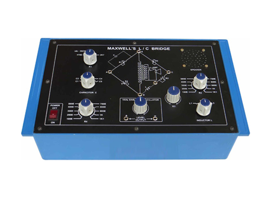
Code:EET0371
Experimental Training Board has been designed specifically for the study of Maxwell's L/C Bridge. Using this bridge the value of unknown capacitor or an unknown inductor can be found. The board is absolutely self contained and requires no other apparatus.
Practical experience on these boards carries great educative value for Science and Engineering Students.
Object:
- To measure value of unknown capacitance.
- To measure value of unknown Inductance.
Features:
The board consists of the following built-in parts :
- ±12V D.C. at 100mA, IC regulated Power Supply internally connected.
- 1 KHz Sine Wave Oscillator.
- Audio Amplifier and speaker for null detection.
- Five unknown values of capacitors selectable by a band switch.
- Three unknown values of inductors selectable by a band switch.
- Two decade resistances in 100 ohm steps.
- Potentiometer and adequate no. of other electronic components.
- Mains ON/OFF switch, Fuse and Jewel light.
- The unit is operative on 230V ±10% at 50Hz A.C. Mains.
- Adequate no. of patch cords stackable from rear both ends 4mm spring loaded plug length ½ metre.
- Good Quality, reliable terminal/sockets are provided at appropriate places on panel for connections/observation of wave forms.
- Strongly supported by detailed Operating Instructions, giving details of Object, Theory, Design procedures, Report Suggestions and Book References.
- Weight : 3 Kg. (Approx.)
- Dimension : W 340 x H 110 x D 210
Note: Specifications are subject to change. Order Code can be different from Manufacturer's Model No.


